Development of a Silicon Retinal Implant: Microelectronic
System for Wireless Transmission of Signal and Power
I. Abstract
Purpose. To develop a method of wireless communication to
supply power and signal (visual scene detail) to an epiretinal
prosthesis.
Methods. In this system, now partly built and electronically
tested, an external laser provides signal and power to the implant.
An 820nm laser beam enters the eye, illuminates an internal
photodiode array, powering the microchip upon which the array is
mounted. Chip circuitry interprets small, rapid intensity
variations, deliberately modulated on the laser beam to encode scene
detail, and uses them to determine the location, duration and
intensity of electrical stimulation passed to retina through a dense,
implanted microelectrode array.
Results. A 12-cell phototdiode array, 2.2 mm square, was
fabricated. Its power efficiency of 18% is adequate to power the
chip with a 1W/sqcm beam, weak enough to avoid retinal damage at this
wavelenth. The array was then attached to a glass covership and
electrically isolated via a saw-etch technique. The chip, which was
fabricated in a 214 CMOS process, consists of about 10,000 transitors
and occupies a 2.2mm X 2.2mm area. The voltage and currrent
regulators, high frequency filters, logical cuircuits, and electrode
drivers function as expected, but the reference circuits need
additional buffering and a slightly modified design is under
fabrication.
Conclusions. Test results indicate that needed functionality
can be achieved within power and area budgets. The modified circuit
for the epiretinal prosthesis should be available for experimental
implantation in 1994.
II. Introduction
This research is part of the Retinal Implant Project, a collaborative
effort of the Massachusetts Eye and Ear Infirmary and the
Massachusetts Institute of Technology. The goal is to develop an
independently functioning, epiretinal prosthesis to restore vision to
patients with disease of the outer retina, especially retinitis
pigmentosa and macular degeneration. This poster represents work
within one of the seven areas of the overall research effort.
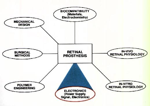
Figure 1
Design goals include placing as few components as possible within the
eye and providing power and signal to the implant without having to
penetrate the eye with wires (Figure 2). The design achieves these
ends by:
- Capturing the visual scene with a tiny CCD camera mounted
on eyeglasses,
- Encoding the image in small variations in the beam
intensity of an externally mounted laser,
- Tranmitting the processed beam to the microchips implanted
within the eye, adjacent to the retina.
Combining Power and Signal Components for Optical
Transmission to Retinal Implant Circuit
The small, external laser (820 nm) is powered by a battery and its
output modulated by a pulse stream from the CCD sensor, which
represents the visual scene. The modulated laser output is incident
on the intraocular photodiode array (Figures 3-4), which generates
the electrical supply voltage. This electrical supply powers the
stimulator circuitry (see next panel, central). Variations in the
incident laser beam are first read by the signal photodiode, then
transferred to and decoded by the stimulator chip and finally used to
control the location and timing of electrical pulses. The pulses are
sent to the flexible electrode array which sits in curved position
against the retina.
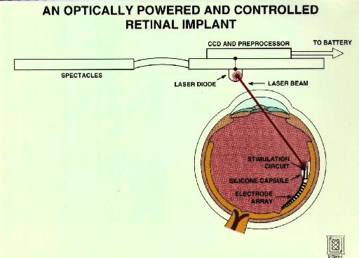
Figure 2
An Optically Powered and Controlled Retinal Implant
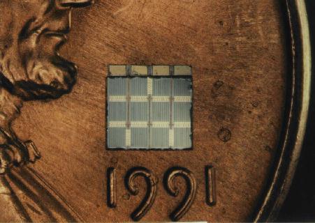
Figure 3
Top surface of twelve-cell photodiode
array, which powers the stimulator chip.
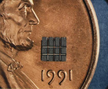
Figure 4
Back surface of the photodiode array. This view demonstrates the
sawed incisions that are used to prevent current leakage between
cells.
Transmission of Power and Signal on a Single Laser Beam
As indicated in Figure 5, the overall beam intensity (blue) is
sufficient to drive the implanted photodiode array and power the
stimulator chip. Details of the visual scene are encoded in the
pulse stream by superimposition of an amplitude modulated signal
(orange) upon the DC laser output. The modulated signal is detected
by an internal signal photodiode that converts the optical signal
into the electrical input to the stimulator logic. The logic
controls current sources that excite the electrodes, which produce a
pattern of biphasic pulses intended to stimulate the retinal ganglion
cells with a spatial pattern representative of the initially viewed
30 image incident on the CCD sensor.
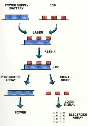
Figure 5
For Preliminary Experiments, This Curcuit Stimulates
all Electrode Simultaneously
The laser light waveform allows independent control of the output by
carrying the following information (see Figures 6-8):
- amplitude of the anodic pulse -- given by sampling the input
level during the anodic stimulation period.
- amplitude of the cathodic pulse.
- beginning and end times of the anodic pulse -- determined by the
time between the first two positive pulses.
- beginning and end times of the cathodic pulse -- determined by
the second pair of positive pulses.
- the reset that begins a new cycle -- initiated by the first
negative pulse.
- elimination of accumulated electrode charge by shorting the output to a
reference voltage -- initiated by the second negative pulse.
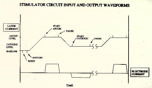
Figure 6
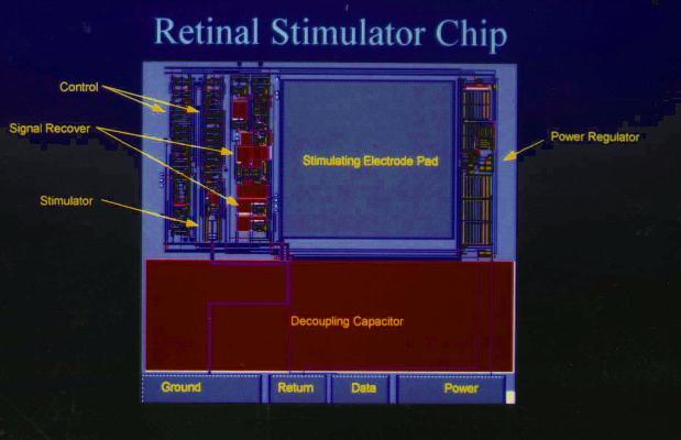
Figure 7
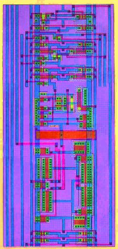
Figure 8
Stimulator Chip
The stimulator chip (Figure 9) recognizes variations in the signal
diode output that represent beam intensity fluctuations due to the
encoded visual signal. These variations drive a small finite state
machine that in-turn drives the electrodes cathodically or
anodically, or alternatively crreates open circuits or shorts between
the electrodes. Beam intensity governs the strength of cathodic and
anodic stimulation.
Expanded view of delay circuit (Figure 8), representing a region
about 1/2 inch in length in the layout of the stimulator chip (Figure
7). Each transistor (red strip surrounded by green on both sides) is
laid out by hand. The thin red polysilicon lines are 2 microns in
width.
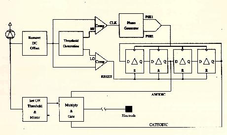
Figure 9 Block Schematic of Stimulator Circuit
The implant consists of a thin, flexible polimide electrode array
sandwiched between two silicon microchips (Figure 10). The upper
chip contains the photodiode array and signal diode, which supply
electrical power and visual signal information to the underlying
stimulator chip (i.e., drive circuit).
Cantilevered polyimide electrode array (Figure 1 1). The
prototype implant contains only twenty electrodes (shown at the top)
and these electrodes are wired in parallel to provide simultaneous
stimulation. The seven possible contact points allow a variety of
choices for total lenght of the array.
Enlarged view of several electrodes (Figure 12). Each is 25
microns in diameter and has been plated with platinum black, which
reduces electrical resistance and increases surface area (which
reduces the local concentration of toxic electrochemical byproducts).
Monolithic Silicon Stimulator
The present retinal stimulator apparatus is a hybrid structure using
thin metallized polyimide for the electrode array, which is
wire-bonded to a silicon integrated circuit that is connected in turn
to the optically powered supply source. For implants comprising
thousands of stimulating electrodes, a fully monolithic structure
built from thinned silicon is the best solution to forming the large
number of electrodes that must be connected to the stimulating
electronic circuit.
Figure 13 shows a mechanical model of thinned silicon in which
the cantilevered area that would contain the electrode array is only
12 microns thick, and the circuit area is 75 microns thick. The
black rectangle below was used to mask the circuit area during final
thinning of the array.
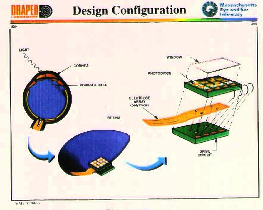
Figure 10 Design Configuration
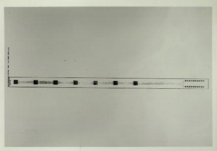
Figure 11
Figure 12
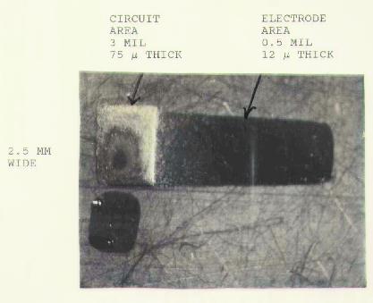
Figure 13
Figure 14
III. Discussion
The design of the electronic system provides three significant
benefits:
1. Minimizes the amount of electronics that need to be placed in
the eye
The risk of electronic failure is partially related to how much
electronics is placed into the eye. The eye is basically a hostile
environment for electronics -- even minute quantities of salt will
destroy the chips, Also, faulty internal components could only be
changed by undertaking additional surgery. Therefore, it is
desirable to internalize only those components that absolutely need
to be intraocular.
2. Permits changes to be made in the signal drive without having
to perform additonal surgery
It can be safely assumed that whatever stimulation strategies are
chosen, perception will not likely match our expectations. The
ability to alter the function of the internal chip without entering
the eye is a great advantage. New developments in image coding can
be used to upgrade the system. Patients can provide feedback that
could be used to individualize the stimulation protocol.
3. Eliminates the need for wires
Both signal and power are provided by the invisible laser light.
Radiofrequency could also be used to provide both signal and power,
but light offers the advantage that much greater volume of data can
be transmitted. Infrared light is also advantageous in that the 820
nm wavelength is just above the bandgap of silicon, which means
optimum efficiency for energy transfer. This higher efficiency
reduces the intensity of light needed to power the chip, which
lessens the risk of light-induced retinal damage.
The electronic design also includes low-power circuitry, which
was specially designed for this project. The lowered energy demand
lessens the amount of energy that needs to be transmitted into the
eye, and proportionately increases the amount of current that can be
delivered to the electrodes. This luxury potentially increases the
number of electrodes that can be driven by a given amount of energy
entering the eye.
The chip also has a fairly unique property. When there is a
"power failure", as will occur with each blink of the eyelid, the
chip shuts down in a known state. When power is restored, the chip
begins to function in that known state (without having to "reboot"),
which improves its efficiency.
IV. CONCLUSION
- The most serious challenge facing this project is the
uncertainty of biocompatibility at the neural-electrode interface.
- Both signal and power can be transmitted to internal components
without wires.
- Sufficient power can be transmitted with a relatively low
intensity of infrared light to drive 20 electrodes, which should be
more than adequate to produce a retinal response that we can detect
by recording from subdural electrodes positioned over the visual
cortex (see our adjacent poster # 592-40).
- All electronic components have been designed, manufactured and
tested. Invivo testing of the retinal prosthesis will begin shortly.